FPGA Hardware Resources: LUTs, BRAM, DSP, Clocking, and Routing
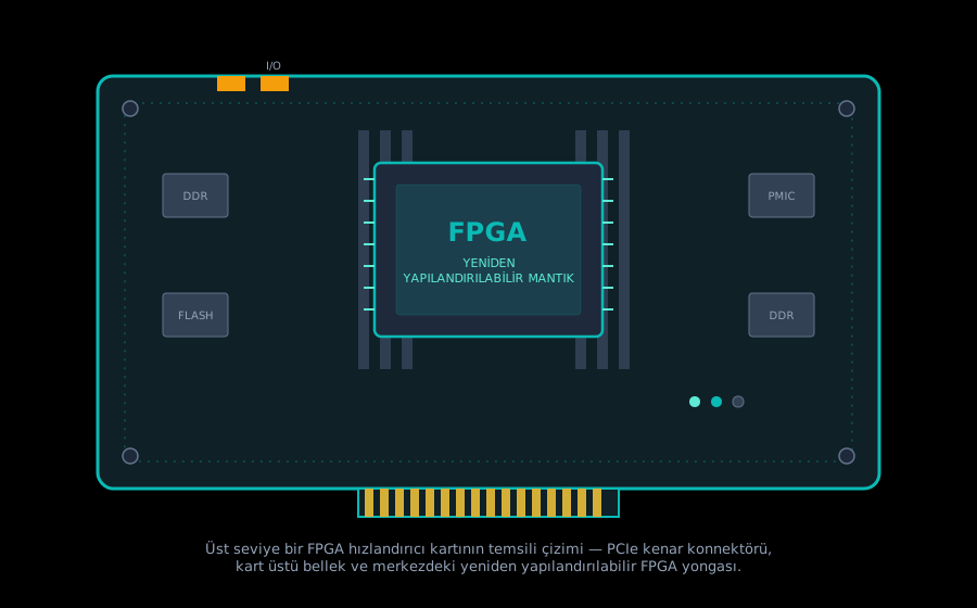
FPGA Hardware Resources: LUTs, BRAM, DSP, Clocking, and Routing
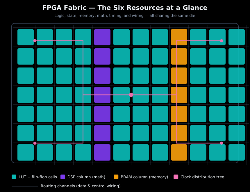
Last time we talked about why FPGAs matter flexible hardware that reshapes itself for the job. This time we open up the fabric and look at what that flexibility is actually made of. Strip awQay the marketing diagrams and every FPGA is built from the same five kinds of resources, wired together on one die.
LUTs, the programmable logic
A LUT (Look-Up Table) is the smallest unit of decision-making logic on the chip a tiny truth table you can reprogram. Give it a few inputs, and for every combination of those inputs, the LUT has one bit of memory saying what the output should be. Set those memory bits once, when the chip loads its bitstream, and the LUT behaves exactly like a fixed logic gate AND, OR, XOR, or anything else until you reconfigure it. Depending on the architecture, a LUT can have anywhere from 4 to around 8 inputs; most modern FPGAs settle on 4- to 6-input LUTs as the sweet spot between how much logic one LUT can absorb and how much silicon it costs.
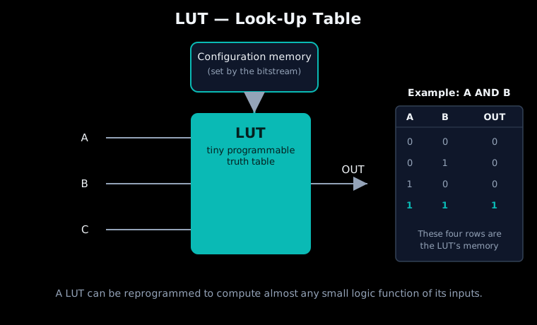
Thousands of these tiny truth tables, each independently programmed, are what let the same chip become a counter one day and a filter the next.
Flip-flops, the memory of the fabric
A LUT decides, a flip-flop remembers. Each flip-flop holds a single bit and updates it only on a clock edge, which is what turns a pile of combinational logic into a pipeline, a counter, or a state machine. They sit directly beside the LUTs in most architectures every LUT output has one or two flip-flops available to it, because almost every LUT in a real design feeds one.
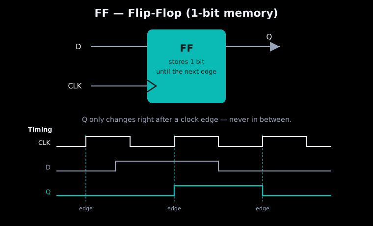
Flip-flops are also the reason timing analysis exists. Every path the tool checks runs from one flip-flop, through some LUTs and routing, into the next flip-flop, and the clock period has to be long enough for the slowest of those paths. Adding flip-flops shortens each path: that is precisely what pipelining means in hardware.
BRAM & DSP, the two hard-wired workhorses
LUTs are flexible, but flexibility has a cost building large memories or fast multipliers purely out of LUTs is slow and eats up huge amounts of fabric. So every FPGA also ships two kinds of purpose-built, hard-wired blocks sprinkled through the fabric.
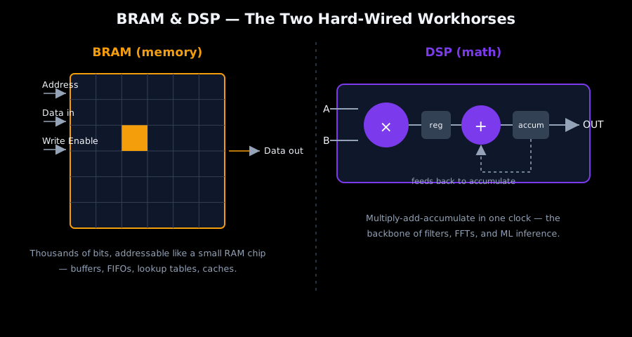
BRAM (Block RAM) is a self-contained memory array baked into the chip give it an address, and it hands back or stores the data there on the next clock edge. A single BRAM instance typically holds somewhere around 18 to 36 kilobits, depending on the architecture, and organizes those bits into whatever width your design asks for wide and shallow, or narrow and deep. It’s what buffers, FIFOs, lookup tables, and caches are built from, without spending a single LUT.
DSP slices are hard-wired multiply-add-accumulate units. Instead of building that math out of general logic which would be both slower and far more expensive in area a design just uses one of these pre-built blocks directly. A single DSP slice can multiply two fairly wide operands commonly somewhere in the range of 18 to 27 bits per input and accumulate the result, all in one clock cycle, at a fraction of the LUT cost that the same multiply would take if built from scratch. That’s why FPGAs are so good at filters, FFTs, and machine-learning inference: the math-heavy part of the job runs on silicon built specifically for it.
Clocking & Routing, the two networks that tie it together
Logic, memory, and math blocks are useless in isolation. Two more networks thread through the whole chip to make them work together: one carries the clock, the other carries everything else.
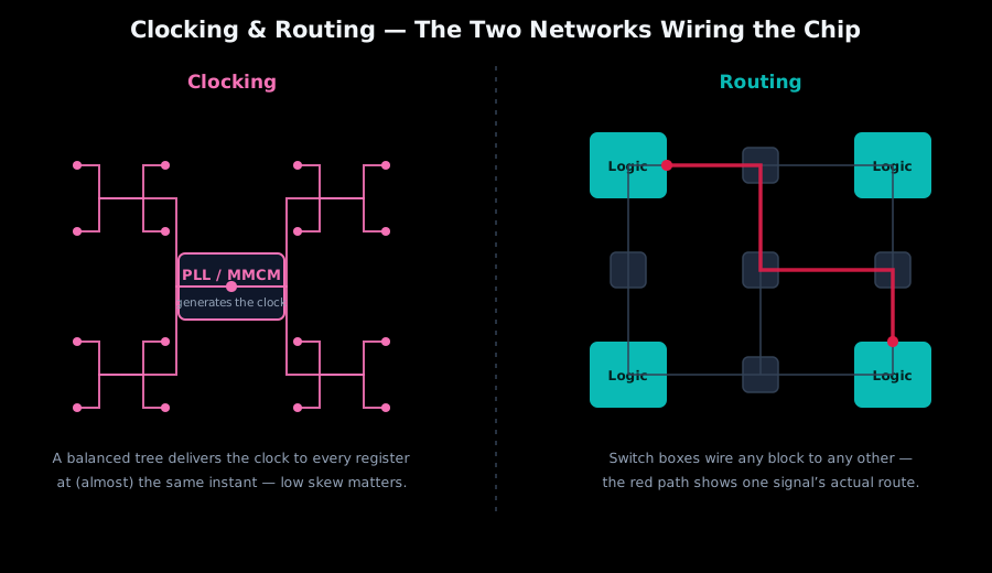
Clocking starts at a PLL or MMCM, which takes an input clock and generates the precise frequencies the design actually needs. From there, a carefully balanced tree distributes that clock to every register on the chip so they all update at (almost) exactly the same instant. That “almost” matters the tiny timing difference between when the clock arrives at different registers is called skew, and too much of it is one of the most common ways a design fails to hit its target speed.
Routing is the general-purpose wiring: a dense mesh of programmable wire segments with switch boxes at every intersection. To connect one block’s output to another block’s input, the place-and-route tool finds a path through this mesh and configures each switch box along the way. Longer, more congested routes are slower which is why where your design’s blocks land on the chip affects performance just as much as the logic itself.
Quick Recap
| Resource | What it does |
|---|---|
| LUT | Computes a small, reprogrammable logic function |
| Flip-flop | Holds one bit of state, updating on a clock edge |
| BRAM | Stores data on-chip as addressable memory |
| DSP | Hard-wired multiply-add-accumulate math |
| Clocking | Distributes a synchronized timing signal to every register |
| Routing | Programmable wiring connecting every other resource |
Every FPGA design, no matter how complex, ultimately breaks down into some combination of these six things. Next time you open a utilization report and see LUT count, flip-flop count, BRAM count, DSP count, and a timing summary, you’ll know exactly what’s being counted, and why it matters.
These six are the fabric itself, but they are not everything on the die. Around the edges sit I/O banks that drive the physical pins, and on larger parts high-speed serial transceivers for protocols like PCIe and Ethernet. SoC devices go further still, placing hard PCIe and memory controllers and full ARM processor cores on the same piece of silicon as the fabric.
One Level Deeper: Fracturazation
There’s a trick underneath all of this that makes these resources even more flexible than they first appear: fracturing. Instead of a LUT, DSP, or BRAM only being usable as one big fixed block, many FPGA architectures let a single large primitive split “fracture” into two or more smaller, independent resources when your design needs more small pieces instead of one big one. It’s an extra layer of reconfigurability sitting on top of the reconfigurability we already talked about, and it’s a big part of why FPGA utilization numbers are more nuanced than a simple resource count.
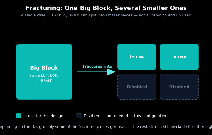
A fracturable LUT is typically built as one larger look-up table that can either operate as a single wide function, or be split into two smaller, independent functions with fewer inputs each as long as they share some of the same input pins. Which mode gets used is decided automatically by the synthesis tool, based on whichever packs your logic more efficiently.
DSP slices can fracture too. A single large DSP block built for one wide, high-precision multiply can often be reconfigured to instead perform several smaller, lower-precision multiplies in parallel which is especially valuable for workloads like low-precision AI inference, where many narrow multiply-accumulate operations matter more than a few wide ones. (The exact split varies by vendor and DSP generation, so always check your specific architecture’s documentation for the precise numbers.)
BRAM can be fractured along similar lines for example, one larger memory block can potentially be split into two smaller, independent memories, each with its own address and data ports, when a design needs more independent memory ports rather than one larger contiguous space. (Caveat: BRAM fracturing details vary quite a bit by vendor and family, so treat this as the general idea rather than a specific number.)
The pattern underneath all three examples is the same one you’ll see again and again in FPGA architecture: a big, capable block is designed so it can fracture and break down into a few smaller, independent blocks whenever the design calls for more of the smaller kind rather than one of the larger kind. It’s a small architectural idea with an outsized effect it lets a fixed number of physical primitives on the die serve a much wider range of designs than a rigid, one-size resource ever could.
Summary
We don’t optimize for utilization. We optimize for the margin that survives the next requirement change. That is a different design decision, and usually a different architecture: the build that wins on LUT count today is often the one that gets rewritten when the spec moves, a wider payload, one more mode, a second clock domain. Headroom that exists in only one configuration was never headroom but a smart design practice.