What Is an FPGA? A Practical Guide | RunX Technology
What Is an FPGA?
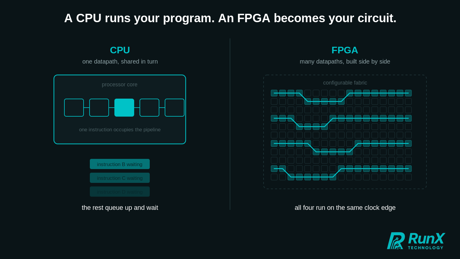
A CPU runs your program. An FPGA becomes your circuit.
That single sentence is the whole idea, and almost everything else follows from it. But it is also the part that most explanations skip, which is why engineers new to the field often come away thinking an FPGA is just an unusually awkward processor. It isn’t. It is a different answer to a different question.
This article opens a series we are publishing through the rest of the year, in which our engineers go deep on individual topics: hardware resources, verification, high-speed interfaces, signal processing, edge AI. Before any of that, it is worth being precise about what an FPGA actually is.
A field of logic, not a sequence of instructions
FPGA stands for Field-Programmable Gate Array. Unpack it backwards and the name explains itself: an array of logic that can be configured in the field, after the chip has been manufactured.
Inside the device is a fabric of small, generic building blocks:
- Lookup tables (LUTs) - tiny configurable truth tables, typically with four to six inputs, that can implement any Boolean function of those inputs.
- Flip-flops - single-bit storage elements that hold state between clock edges.
- DSP blocks - hardened multiply-accumulate units for arithmetic-heavy work.
- Block RAM - on-chip dual-port memory, distributed across the fabric.
- Clocking resources - PLLs and dedicated clock networks that distribute timing across the device.
- I/O and transceivers - from simple pins to multi-gigabit serial links.
None of these blocks does anything useful on its own. What makes an FPGA an FPGA is the programmable interconnect between them: a switching network that decides which block connects to which. When you configure the device, you are setting millions of these switches at once, using a file called a bitstream.
The result is not a program the device executes. It is a circuit the device has become.
This is why “programming an FPGA” is a slightly misleading phrase. What you actually write, in VHDL or SystemVerilog, is a description of hardware - a specification of registers, datapaths, state machines and their timing relationships. A synthesis tool maps that description onto the available LUTs, flip-flops and DSP blocks, and a place-and-route tool decides where each piece physically sits and how signals travel between them. The mental model is closer to architecture than to coding.
Space instead of time
Here is the shift that takes the longest to internalise.
Software gets its work done over time. A processor has one set of arithmetic units, and instructions take turns using them. Want to do more? Take more clock cycles, or add more cores and share differently.
An FPGA design gets its work done in space. If you need eight multiplications simultaneously, you instantiate eight multipliers and they all run on the same clock edge. If a filter, a decoder and a control loop must operate at once, each occupies its own region of the fabric and none waits for the others.
Two consequences are worth stating plainly.
The first is determinism. A pipeline clocked at 200 MHz produces a result every 5 nanoseconds - every sample, every frame, every time. There is no cache to miss, no scheduler to preempt you, no other tenant competing for the same execution units. Latency is not something you measure afterwards and hope holds; it is something you calculate up front and then prove with static timing analysis. In safety-critical and mission-critical systems, that provability is often the entire reason an FPGA is in the design.
The second is that resources are finite in a very physical way. You cannot add a loop for free. Every function you add consumes LUTs, DSP blocks or memory that something else can no longer use. Good FPGA engineering is largely the discipline of budgeting - logic, memory bandwidth, and above all timing.
FPGA, CPU, GPU, ASIC: choosing honestly
These four are not competitors so much as different points on a trade-off surface.
| Strength | Weakness | Typical fit | |
|---|---|---|---|
| CPU | Flexible, fast to develop, rich software ecosystem | Sequential; worst-case timing hard to bound | Control, orchestration, user interfaces |
| GPU | Enormous parallel throughput | Reaches that throughput by batching, which hurts latency; high power | Training, offline batch processing |
| FPGA | Deterministic timing, true parallelism, rich I/O, reconfigurable after deployment | Higher engineering effort; lower clock rates than ASICs | Real-time signal processing, sensor interfacing, low-latency inference |
| ASIC | Best performance, power and unit cost at volume | Very high non-recurring engineering cost; no flexibility once fabricated | High-volume products with frozen requirements |
The comparison people usually get wrong is FPGA versus GPU for AI. A GPU will win on raw throughput almost every time. But throughput and latency are different currencies. A GPU reaches its advertised numbers by batching work, and in a batch the first item waits for the last. If your requirement is “classify this frame within 2 milliseconds, every frame”, batching is the problem, not the solution.
The comparison that matters commercially is FPGA versus ASIC. An ASIC beats an FPGA on power, speed and per-unit cost - but only after you have paid the non-recurring engineering cost, which on modern process nodes runs into millions, and only if your requirements never change. FPGAs win the middle ground: moderate volumes, long product lifecycles, evolving standards, and any programme where a specification might still move.
Every chip in that table is an RTL design
There is something the comparison hides, and it matters more than the comparison itself.
A CPU is an ASIC. So is a GPU. Neither arrived in the world as a finished object. Each began as a description written in VHDL or SystemVerilog by digital design engineers, verified in simulation, synthesised, placed, routed, and finally committed to silicon. The register-transfer level description is the common ancestor of every device in that table.
Two things follow from this.
FPGA design and ASIC design are the same discipline aimed at different targets. Architecture and pipelining, clock-domain crossing, resource and timing budgeting, verification methodology, timing closure - these are not FPGA techniques. They are digital design techniques. The target changes what you optimise for; it does not change the craft. An engineer who can close timing on a demanding FPGA design is doing the same work that produced the processor in your laptop.
FPGAs are how ASICs get de-risked. Before committing to a mask set - a decision measured in millions of dollars and many months, with no undo - teams map their RTL onto large FPGAs or FPGA-based emulation platforms and run real software against the real design. A bug found there costs engineering time. The same bug found after tape-out costs a respin. This is why FPGA prototyping is a standard stage in serious silicon programmes rather than an optional extra.
The same logic applies commercially. Plenty of products ship first as an FPGA and harden into an ASIC only once volumes justify the investment - the same RTL, retargeted. The FPGA is not the compromise version of the ASIC; it is the stage the ASIC has to pass through.
So when a team says it has FPGA capability, that is not a narrow specialisation. It is the ability to design digital hardware - the skill that produced everything else in the table.
The price objection
FPGAs carry a reputation for being expensive. It is worth separating where that reputation is earned from where it is not.
The devices span an enormous range. At the top sit large parts with hundreds of gigabit transceivers and integrated high-bandwidth memory, costing thousands of dollars each - and these are the devices people tend to picture when they hear the word FPGA. At the other end sit small devices with a few thousand to a few tens of thousands of logic cells, no high-speed serial, modest I/O. Those sell for single-digit dollars in volume, which places them in the same band as a mid-range microcontroller. Some of the smallest are cheaper than the microcontroller they would replace.
So “is an FPGA expensive?” is not really a question about FPGAs. It has the same shape as asking whether a processor is expensive - the answer depends entirely on which one, and choosing the smallest device that meets the requirement is a core part of the design work.
Where the reputation is earned is engineering. Tool licences for the larger device families are not free. Board design is more demanding - power sequencing, configuration memory, more careful signal integrity. And above all, design and verification take real effort, with verification typically the larger share.
That is the honest trade. On a small programme the device is rarely the dominant cost; the engineering is. Knowing that before you budget for a first FPGA project is the difference between a project that lands and one that surprises you.
Signals that your problem wants an FPGA
In our own work, the same handful of indicators keep appearing.
A deadline you cannot miss. Flight control loops, weapon safety interlocks, motor commutation, radar processing windows. Where “usually fast enough” is not an acceptable answer.
Data arriving faster than a processor can accept it. High-rate ADCs and DACs over JESD204B, image sensors over MIPI, video over SDI, sensor fusion across multiple simultaneous streams. FPGAs sit closest to the physical layer, which is often exactly where the bottleneck is.
A protocol that no chip implements for you. Custom or legacy interfaces, proprietary bus formats, unusual timing requirements. This is where an off-the-shelf part simply does not exist.
A standard that is still moving. If the specification may change after hardware ships, reconfigurability is not a nice-to-have - it is what saves the programme.
Power-constrained inference at the edge. Quantised neural networks mapped onto fixed-point datapaths can deliver useful accuracy within a few watts, which is often the difference between a system that flies and one that does not.
Component longevity. Defence and aerospace programmes measure lifecycles in decades. FPGA vendors support devices far longer than most processor lines, and a design that is portable across vendors is insurance against supply-chain disruption.
What an FPGA project actually involves
One honest note, because expectations here are frequently wrong: writing the RTL is not the bulk of the work.
A typical programme runs through requirements capture, architecture and resource budgeting, RTL implementation, functional verification, timing closure, then board-level integration and test. Verification routinely consumes more effort than design - and in DO-254 or similar assurance contexts it dominates, because every requirement must be traceable to a test that demonstrably passes.
That is not overhead. It is the reason the deterministic guarantees hold in the field rather than only in simulation.
Where this series goes next
Over the coming weeks our engineers will take these topics apart one at a time: the hardware resources inside the fabric, how processor and logic coexist in SoC devices, how to choose a device family, verification methodology, high-speed interfaces, image and radar signal processing, and edge AI.
At RunX Technology we design FPGA and SoC systems where timing is engineered rather than hoped for - from IP cores and video pipelines to radar signal processing and DO-254 verification. If you have a problem with a deadline attached to it, that is the kind we like.
Talk to us: info@run-x.com | www.run-x.com