PS and PL Architecture in FPGA SoC Devices

On FPGA SoC platforms deciding whether a task should be handled by the processor or the FPGA is not a mere preference, but a fundamental architectural decision. That is because the chip in your hands is not just an FPGA: a quad-core ARM processing system (PS) and programmable logic (PL) sit on the same silicon, and the data path between them is yours to build.
On paper the split looks easy: “fast things to the PL, easy things to the PS.” In a real project, though, that split directly determines latency, bandwidth, CPU load and how far the system can grow. A single block sitting on the wrong side can slow down the whole chain.
In this article we take the radar focused architecture we developed on the FPGA as an example and cover three things: the rule we used to divide the work, how we moved the data from the ADC to DDR4, which AXI interface we chose and why.
What Does an FPGA SoC Change Compared to a Classic FPGA?
In a classic FPGA design, everything is built on the programmable logic. If you need a user interface, network communication or a file system, you have to write all of it in RTL. That can stretch an ordinary task like “send the output over Ethernet” into weeks of work.
With an FPGA SoC, the equation changes. Linux runs on the PS side: the TCP/IP stack, SSH, the file system, the driver infrastructure and the C/C++ application layer all come ready. The PL side, meanwhile, focuses on what it is good at: parallel computation, deterministic timing, high speed interfaces and clock accurate data processing.
The practical upshot is that you can implement the same function at two very different costs. Sending the radar output to the network is a few hundred lines of socket code on the PS side; building the same thing in the PL with a MAC and a TCP state machine is a sub-project in its own right. Conversely, applying a window to every incoming sample with a fixed latency is natural in the PL, while on the PS it cannot be guaranteed because of operating system interrupts.

The Task Split Between PS and PL
In radar applications, the data rate coming from the sensors is quite high. Running every operation on the ARM processors alone is therefore not an efficient approach. One of the most important advantages of the FPGA SoC architecture is that it lets you distribute tasks properly between Processing System (PS) and Programmable Logic (PL).
In our radar project, we planned the division of work as follows:
| Processing System (PS) | Programmable Logic (PL) |
|---|---|
| YOCTO based operating system and system services | Real-time, per-sample processing of the radar stream |
| Loading and configuring the PL bitstream | AXI4-Stream based signal processing chain |
| Ethernet / TCP-IP and other communication interfaces | High-speed transfer to DDR4 via AXI DMA |
| C/C++ user application (track extraction, reporting) | Stream buffering and rate matching with FIFOs |
| Memory management, drivers, remote update | Custom hardware accelerators (Custom IP) |
| Control of the hardware blocks over AXI4-Lite | Deterministic timing and parallel processing |
We applied a single rule when making the call:
If a job needs a timing guarantee or runs on a per-sample basis, it stays in the PL.
If it makes decisions, manages something or talks to the outside world, it moves to the PS.
How Was the Data Flow Designed?
One of the main goals in the project was to move high-speed radar data into memory while putting as little load on the CPU as possible. The data path we followed looked like this.
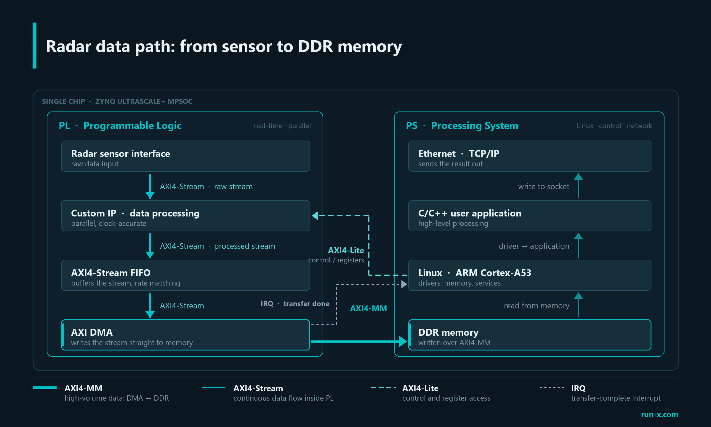
The critical point in this architecture is that the data is processed inside the PL as much as possible, and passed to the PS side only when it needs to be.
That way, the ARM cores can deal with higher level tasks instead of constantly moving data around.
Why Does AXI Matter So Much?
Most of the communication between PS and PL takes place over the AXI protocol.
In FPGA based systems, not every bus serves the same purpose. Depending on what your application needs, you can make use of different AXI interfaces.
AXI4-Lite: Control and Configuration
AXI4-Lite is used for control operations that require little bandwidth. It typically provides register access between the processor and the IP blocks inside the FPGA. You use it to start and stop IP blocks, to update the operating mode and threshold values, and to read status registers.
AXI4-Stream: Continuous Data Flow
AXI4-Stream is designed to transfer data continuously, without carrying any address information. It is the most widely used AXI interface, especially in high-speed data processing applications.
Radar data, camera and video streams, DSP algorithms, and data transfer between IP blocks inside the FPGA all go through this interface.
Because the data packets flow without interruption, it delivers high bandwidth and low latency.
AXI4 Memory-Mapped: Memory Access
The AXI4 Memory-Mapped interface is used when addressable memory has to be accessed. It forms the basis of data transfers between the processor, DDR memory and the DMA controllers. Writing data to and reading it from DDR memory, high-speed transfer via AXI DMA, the processor accessing memory regions on the FPGA, and the storage of large data blocks all run over this interface.
It is the most suitable solution for applications where high volumes of data have to be moved into memory.
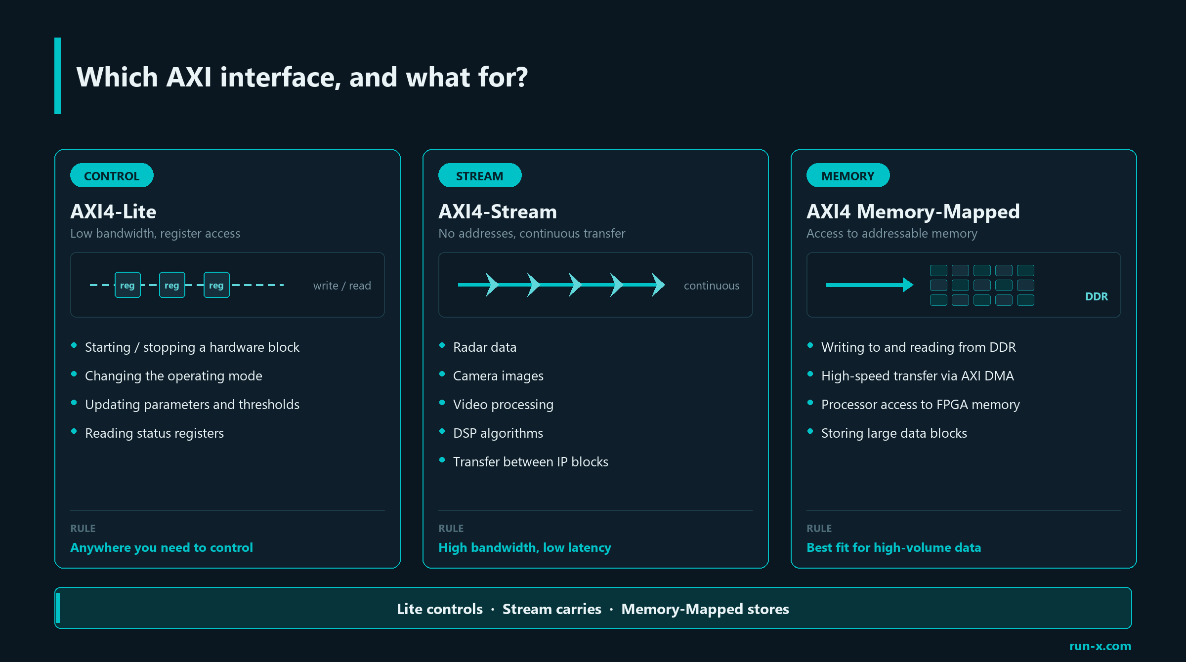
To put all three in one sentence: Lite controls, Stream carries, Memory-Mapped stores.
The Advantage of Using DMA
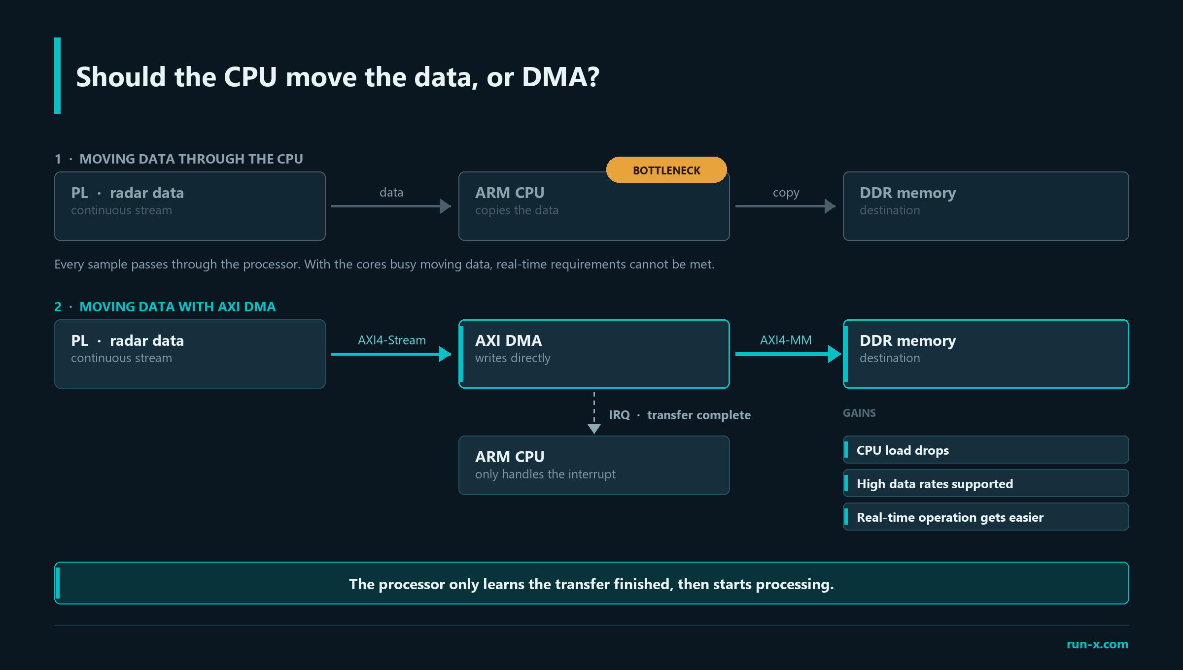
If you move the data through the CPU, it may perhaps work when the volumes are small. In radar applications, though, the data never stops flowing, so the processor on its own falls short of the real-time processing requirements. That is why we chose AXI DMA for the architecture. DMA writes the data straight into DDR memory and so reduces CPU load; because it supports high data rates, it also makes real-time operation easier.
The processor simply learns that the DMA has finished and starts processing the data in memory.
Why Does Linux Run on the PS Side?
Many people wonder why Linux is run inside an FPGA in the first place. The main reason is ease of development. With Linux, TCP/IP communication, SSH access, the file system, application development, remote updates and driver management all become far easier. Sending the radar output to another computer over Ethernet, for example, can be done with standard socket programming on Linux. Doing the same thing purely in FPGA logic would be considerably more complex.
The greatest advantage of FPGA-SoC platforms is not simply that they hold an FPGA and a processor on the same chip. The real power lies in being able to divide the work between these two correctly. That was the basic approach in our radar project as well.
High-speed data processing was carried out on the PL side, while the Linux-based PS side took on system control, communication and application management. Each component did what it is good at, and the system architecture became more modular, more maintainable and easier to extend.
Once you have properly planned where the data comes from and where it goes inside the system, the division of work between PS and PL largely falls into place on its own.
Talk to us: info@run-x.com | www.run-x.com