Requirements Capture & Management for FPGA Projects
Requirements Capture & Management for FPGA Projects
An FPGA can pass every simulation test and still be the wrong design.
A requirement describes what a system or component must do, under which conditions, and within which limits. It gives designers a target and verification engineers a way to check whether that target has been met. If the target is vague, even a well-written RTL implementation may not deliver the intended behavior.
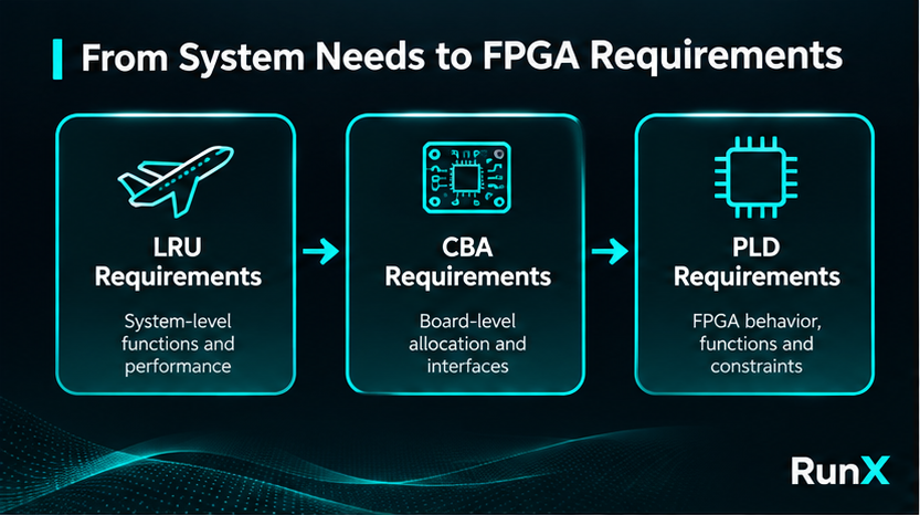
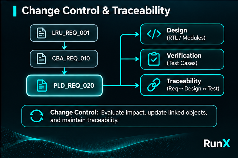
In larger systems, FPGA requirements do not appear in isolation. Functions begin at the system level and are allocated through the equipment architecture—often through a line replaceable unit (LRU) and a circuit board assembly (CBA)—until the responsibilities of the programmable logic device (PLD) are clear. An LRU can also be considered a standalone piece of equipment that performs a specific function within a system or aircraft. A CBA is an electronic board assembly consisting of components mounted on a printed circuit board (PCB) to perform specific functions within an LRU or other equipment. A typical flow is LRU requirements → CBA requirements → PLD requirements. Not every project needs every intermediate level, but the FPGA specification should always reflect what the surrounding hardware actually needs.
Consider a requirement stating that an FPGA must acknowledge a command “immediately.” Does that mean one clock cycle, four cycles, or a fixed number of nanoseconds? The difference seems small until the design team and verification team make different assumptions. Good requirements remove those assumptions before they become RTL.
1. Capture Behavior Before Writing RTL
The most useful FPGA requirements describe what the device must do, rather than how its internal logic should be implemented.
Consider the following examples:
- “The FPGA shall use a three-state finite state machine (FSM) to process commands.” This statement specifies an implementation choice rather than the expected behavior. (✗)
- “The
cmd_ackoutput shall assert high within 1 clock cycle after the following condition is met:- Both
cmd_validandcmd_readyare high at a rising edge ofclk_50.” This statement defines the expected behavior. (✓)
- Both
- “The FPGA shall implement a two-state finite state machine (FSM) to monitor the
fault_insignal and control thefault_outoutput.” This statement specifies an internal design decision rather than the expected behavior. (✗) - “The FPGA shall assert the
fault_outoutput high within 1 clock cycle after the following condition is met:- The
fault_insignal is high at a rising edge ofclk_50.” This statement defines observable and measurable behavior. (✓)
- The
The second and the last statements allow the designer to choose an appropriate architecture while providing the verification engineer with a behavior that can be tested. Of course, additional details, such as the device’s behavior during power-up, reset, and invalid input conditions, should also be defined in the requirements specification.
Start with the FPGA as a Black Box
One practical approach when starting to write requirements is to think of the FPGA as a black box. Begin with its interfaces and consider how each output should respond to inputs, operating conditions, or timing events.
For example, a command controller may have acknowledgment, error indication, and transaction-complete outputs. For each output, consider its expected behavior during power-up, normal operation (assert/deassert), reset, and invalid input conditions.
At this stage, it is important to distinguish between interface definitions and behavioral requirements. For example, defining SCL as the clock line and SDA as the bidirectional data line of the I2C interface, specifying that data is transferred in 8-bit groups, and stating that each data byte is followed by an ACK/NACK bit provide useful interface information. However, this information alone does not describe how the FPGA is expected to behave when communicating through the interface.
Behavioral requirements, on the other hand, define the expected responses of the FPGA outputs under specific conditions. The following is an example of a behavioral requirement:
- “The FPGA shall assert the
tx_doneoutput high within 1clk_i2cclock cycle after generating the STOP condition at the end of an I2C data transfer.”
Such requirements describe not only the characteristics of the interface but also how the FPGA is expected to control its outputs under specific conditions.
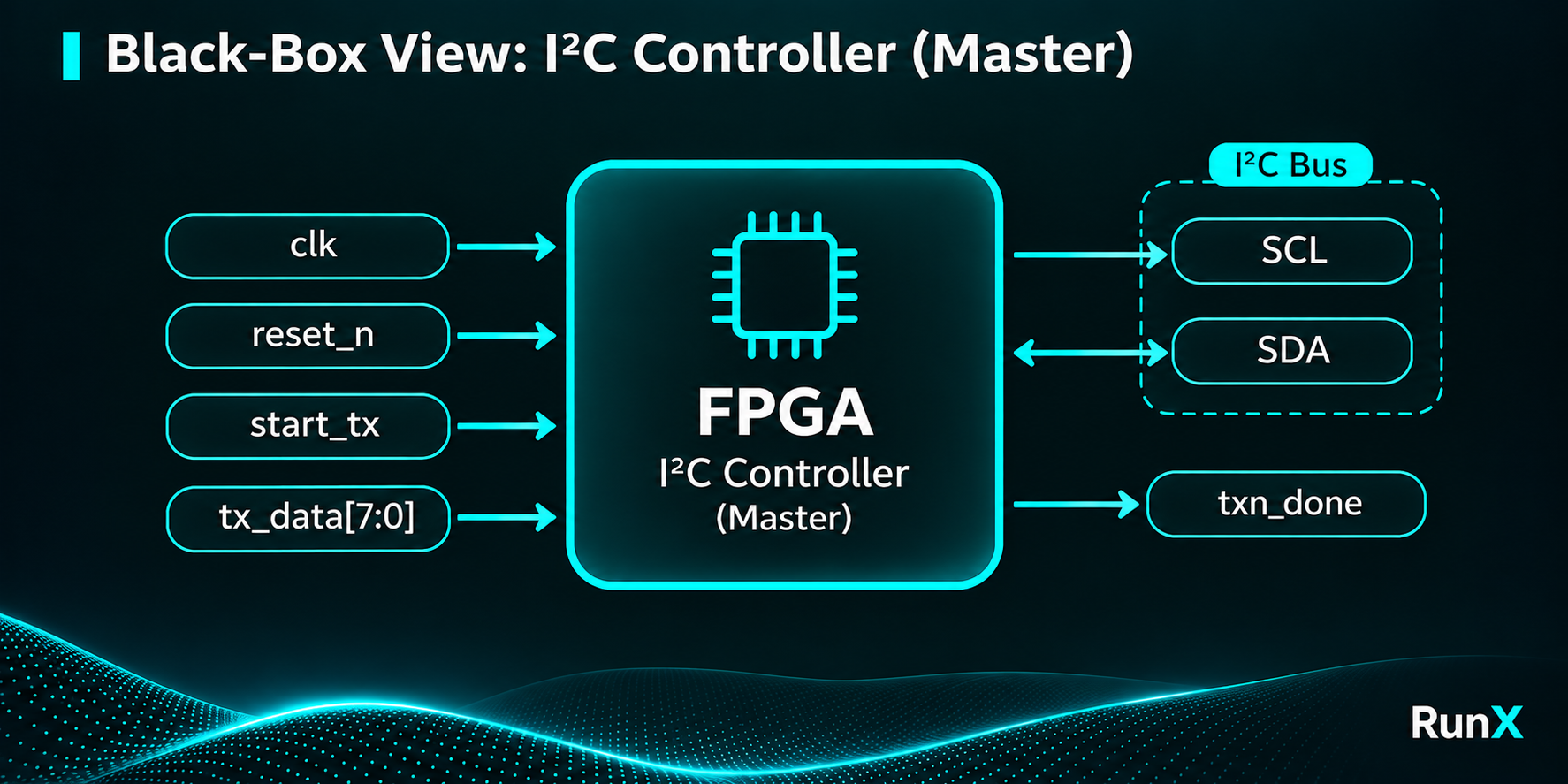
Organizing requirements around outputs and their associated behaviors, an output-first approach, helps keep related requirements together and makes missing or undefined behavior easier to identify. It also provides a useful starting point for requirement-based verification.
However, thinking of the FPGA as a black box does not mean that requirements should be limited to its top-level interfaces. Internal functions, operating constraints, and behaviors that must be defined before implementation should also be captured in the requirements, even when they are not directly observable at the FPGA pins.
Organize Requirements by Function
To make the requirements specification more structured and complete, another useful approach is to identify the main design functions and consider how they might be divided into RTL modules before implementation begins.
This preliminary functional decomposition can serve as a guide for organizing the PLD requirements specification. By grouping requirements under functional headings, engineers can systematically consider what each part of the design is expected to accomplish.
For example, a subsection titled Health Monitoring might contain requirements defining how the PLD shall detect faults, monitor internal status signals, and report error conditions. Similarly, separate subsections could be created for command processing, communication interfaces, or data processing functions, depending on the design.
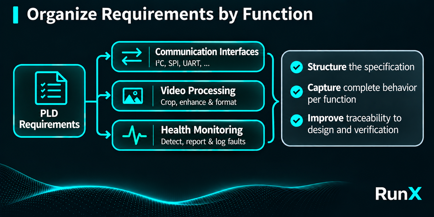
Considering each function individually helps identify behaviors, operating conditions, and dependencies that might otherwise be overlooked. It also makes it easier to establish relationships between requirements, RTL modules, and verification activities later in the hardware design process.
It is important to emphasize that this does not mean the RTL architecture must be finalized during requirements capture. Functional decomposition is intended to support the identification and organization of requirements, not to turn the requirements specification into an RTL design description. Specific implementation constraints should only be included when they are genuinely necessary and justified.
2. Write Requirements That Can Actually Be Verified
A statement containing shall is not automatically verifiable. A strong PLD requirement identifies an observable result, the event that causes it, and any required timing or priority.
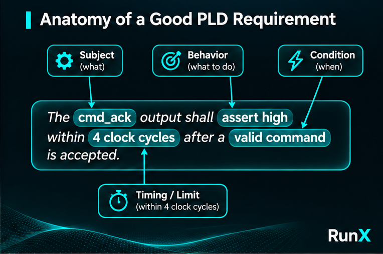
Consider an illustrative command interface running at 50 MHz, where one clock period is 20 ns. First, define valid command as a rising edge of clk_50 on which both cmd_valid and cmd_ready are high. This definition may be an information in the requirements specification. Then write the behavior:
- PLD_REQ_010: The
cmd_ackoutput shall assert high within 4 clock cycles after a valid command is accepted. - PLD_REQ_011: Once asserted,
cmd_ackshall deassert low on the next rising edge ofclk_50. - PLD_REQ_012: When
reset_nis low ,cmd_ackshall be low regardless of the command inputs.
The first requirement establishes a maximum latency of four cycles, or 80 ns. The next two define pulse behavior and reset precedence. The interface specification must also state what happens with overlapping commands or unsupported opcodes if those situations are possible.
These values are illustrative rather than measurements from a customer project. The point is that each statement can produce a clear verification check:
Did the required output occur, after the correct trigger, within the allowed time?
The figure below shows the anatomy of a good PLD requirement.
Timing should come from the application, not the FPGA’s capability.
Suppose the FPGA controls an ADC that transfers a 16-bit serial frame every 2 µs. Sixteen clock periods at 8 MHz take the full 2 µs, leaving no allowance for other protocol timing. At 12.5 MHz, sixteen periods take 1.28 µs. But 12.5 MHz is not automatically the correct requirement: the selected ADC’s data sheet and the board’s sampling needs determine the acceptable frequency range and timing margins.
This distinction prevents a common problem: writing down the timing the current design can achieve rather than the timing the surrounding equipment requires. The same applies to acknowledgment latency, reset recovery, and data-valid windows. State measurable limits and reference events, and avoid terms such as “fast,” “periodically,” or “as soon as possible.”
3. Where DO-254 Fits into Requirements Capturing
The approaches discussed so far are useful for any FPGA project. However, in safety-critical airborne hardware development, writing clear and verifiable requirements is only part of the process. DO-254 provides a structured design assurance framework in which requirements must also be validated, managed, and maintained throughout the hardware design life cycle. AMC 20-152A provides additional guidance and clarifications for its application.
An important distinction in this context is the difference between validation and verification. Validation asks whether the requirements are correct and complete for the intended hardware function, while verification determines whether the implemented FPGA satisfies those requirements. In short:
- Validation: Do these requirements correctly and completely define the intended functions?
- Verification: Does the implemented design meet these requirements?
For example, an FPGA may pass every verification test while implementing a timing requirement that was incorrectly defined in the first place. This illustrates why verifying the implementation alone is not sufficient. It should be noted according to Objective CD-3 of the AMC 20-152A; all requirements whether derived or non-derived, should be validated.
Validation and verification will be covered in more detail in upcoming blog posts.
Requirements Evolve Throughout the Hardware Design Life Cycle
Another important point is that requirements capture is not a one-time activity that ends when RTL development begins. Requirements may be added, refined, or updated throughout the hardware design life cycle, including conceptual design, detailed design, implementation, and verification.
In practice, this is quite common. Design activities may reveal previously unidentified behaviors, constraints, or dependencies, while verification may expose ambiguities or gaps in the existing requirements.
Requirements can be categorized based on their origin and how they are captured at the PLD level:
- Directly Allocated Requirements: Higher-level requirements allocated directly to the PLD without further refinement or decomposition.
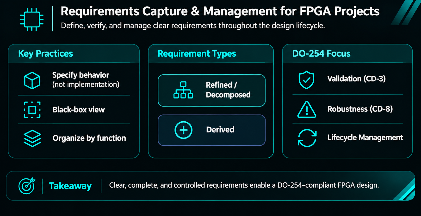
- Refined/Decomposed Requirements: Higher-level requirements refined or decomposed into more detailed PLD-level requirements. These are not considered derived requirements as long as they can be justified by the higher-level requirements.
- Derived Requirements: Additional requirements that cannot be directly traced to higher-level requirements and arise from design decisions, architectural considerations, or implementation needs.
For example, a design decision to introduce an internal fault detection mechanism may lead to additional requirements defining how faults are detected, handled, or reported. These requirements should be documented and validated. In particular, the potential impact of each derived requirement on system safety should be assessed, and the results of these assessments should be incorporated into the relevant system safety processes.
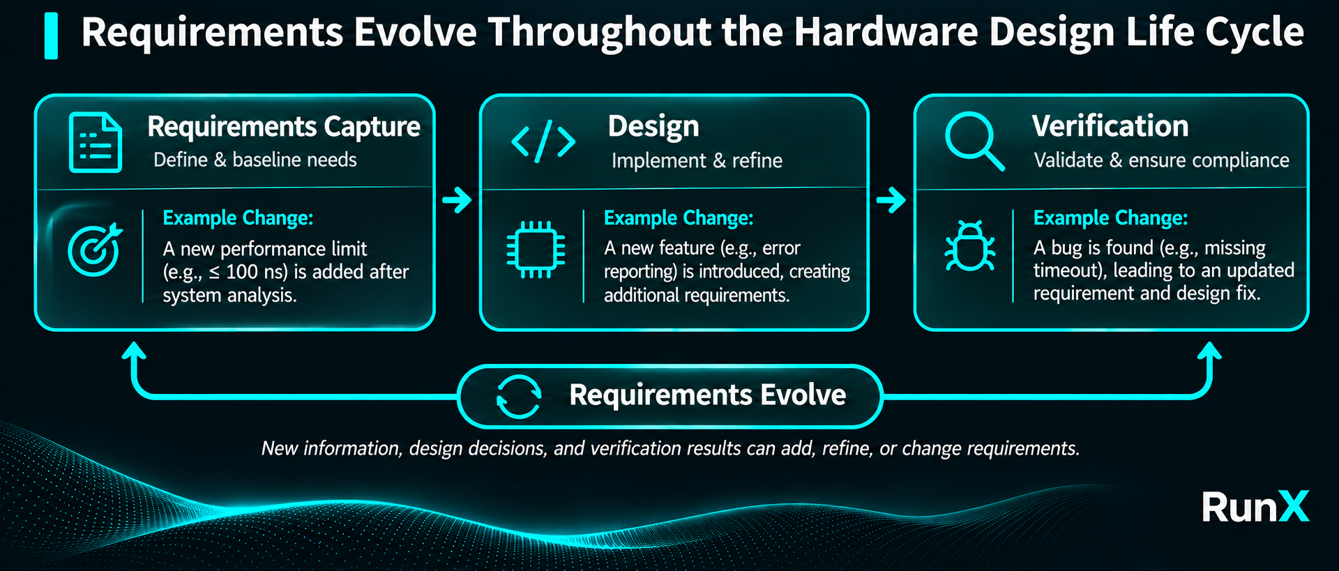
The important point is that requirements are expected to evolve as the hardware design becomes more detailed, but these changes must remain controlled and justified. This is where requirements management, change control, and traceability become essential.
Capturing Abnormal and Boundary Conditions
Under DO-254, requirements should not be limited to the FPGA’s core algorithmic functions. Power-up and post-reset behavior, input/output interfaces and timing constraints, clock and reset relationships, as well as timeout and error conditions should also be addressed. In addition to normal operating conditions, the expected behavior under boundary and worst-case conditions should also be defined.
For DAL A and B hardware, Objective CD-8 addresses abnormal and boundary conditions and their expected behavior. In practical terms, a question such as “What should happen if reset occurs during an active transaction?” should be answered through defined requirements rather than left to incidental RTL behavior. The exact assurance activities depend on the device and applicable project objectives.
Consider an arithmetic operation where two 12-bit unsigned values are added. If the intended behavior is to saturate the result rather than allow wraparound when the sum exceeds the 12-bit range, that behavior should be explicitly specified.
- PLD_REQ_013: When
input_validis high and the unsigned sum ofdata_a[11:0]anddata_b[11:0]exceeds 4095, the FPGA shall setsum_out[11:0]to0xFFFon the next rising edge ofclk_50.
By defining the expected behavior for such conditions, requirements provide a clear basis for both implementation and verification.
4. Make Traceability and Changes Manageable
As discussed in the previous section, requirements may evolve throughout the hardware design life cycle. To manage these changes effectively, engineers must maintain clear relationships between requirements, design elements, and verification evidence.
An example traceability structure can be represented through two separate chains:
- Design Traceability: CBA Requirement → PLD Requirement → Design Element
- Verification Traceability: CBA Requirement → PLD Requirement → Verification Test Case → Verification Result
This structure ensures that PLD requirements are directly linked to both the corresponding design elements and the associated verification activities.
When a requirement is added or modified, these relationships help engineers identify the affected design elements and verification activities, evaluate the impact of the change, and maintain consistency across the project.
Traceability and change management will be covered in more detail in upcoming blog posts.
Closing the Loop
Requirements should be written early enough to guide the design, clearly enough to support verification, and maintained carefully enough to survive change.
Start with the behavior the surrounding hardware needs. Describe PLD outputs in terms of inputs, events, timing, reset, and abnormal conditions. Keep design decisions separate from the functional contract, validate the requirements, and connect every requirement to meaningful evidence.
The goal is not just to show that the RTL works. It is to show that the FPGA performs the function it was built to perform.
Talk to us: info@run-x.com | www.run-x.com
Technical references
- Randall Fulton and Roy Vandermolen, Airborne Electronic Hardware Design Assurance: A Practitioner’s Guide to DO-254.
- DO-254, Design Assurance Guidance for Airborne Electronic Hardware.
- AMC 20-152A, Development Assurance for Airborne Electronic Hardware.